NCP1606
http://onsemi.com
19
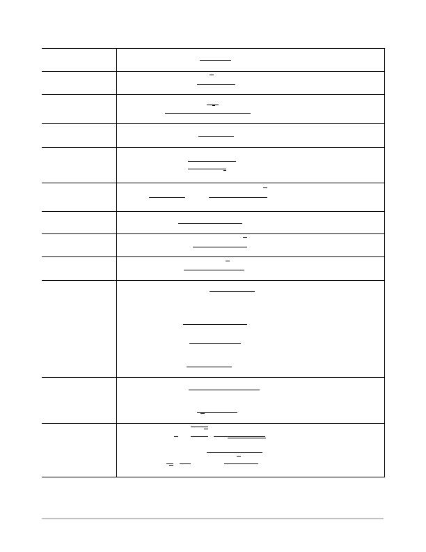
BOOST DESIGN EQUATIONS Components are identified in Figure 1
RMS Input Current
I
ac(rms)
+
P
OUT
h @ V
ac(rms)
h (the efficiency of only the Boost
PFC stage) is generally in the range
of 90 95%
Maximum Inductor Peak
Current
I
pk(max)
+
2 @ 2
@ P
OUT
h @ Vac
LL
I
pk(max)
occurs at the lowest line
voltage.
Inductor Value
L v
2 @ Vac
2
@
V
OUT
2
* Vac
V
OUT
@ Vac @ I
pk(max)
@ f
SW(min)
f
SW(min)
is the minimum desired
switching frequency. The maximum L
must be calculated at low line and
high line.
Maximum On Time
t
ON(max)
+
2 @ L @ P
OUT
h @ Vac
LL
2
The maximum on time occurs at the
lowest line voltage and maximum
output power.
Off Time
t
OFF
+
t
ON
V
OUT
Vac
(rms)
@
sin(q)
@ 2
* 1
The off time is greatest at the peak of
the AC line voltage and approaches
zero at the AC line zero crossings.
Theta (q) represents the angle of the
AC line voltage.
Frequency
f
SW
+
Vac
(rms)
2
@ h
2 @ L @ P
OUT
@1 *
Vac
(rms)
@ |sin q| @ 2
V
OUT
Pin 3 Capacitor
Ct w
2 @ P
OUT
@ L @ I
CHARGE
h @ Vac
RMS
2
@ V
CTMAX
I
CHARGE
and V
CTMAX
are given in
the NCP1606 specification table.
Boost Turns to ZCD Turns
Ratio
N
B
: N
ZCD
v
V
OUT
* Vac
HL
@ 2
V
ZCDH
The turns ratio must be low enough
so as to trigger the ZCD comparators
at high line.
Resistor from ZCD wind-
ing to the ZCD pin (pin 5)
R
ZCD
w
Vac
HL
@ 2
I
CL(NEG)
@ (N
B
: N
ZCD
)
R
ZCD
must be large enough so that
the shutdown comparator is not inad-
vertently activated.
Boost Output Voltage
V
OUT(nom)
+ 2.5 V @
R
OUT1
) R
OUT2
R
OUT2
Maximum V
OUT
voltage
prior to OVP activation and
the necessary R
OUT1
and
R
OUT2
.
V
OUT(max)
+ V
OUT(nom)
) R
OUT1
@ I
OVP
R
OUT1
+
V
OUT(max)
* V
OUT(nom)
I
OVP
R
OUT2
+
2.5 V @ R
OUT1
V
OUT(nom)
* 2.5 V
I
OVP
is given in the NCP1606 spe-
cification table. I
OVP
is lower for the
NCP1606B, then for the NCP1606A
version.
Minimum output voltage
necessary to exit under-
voltage protection (UVP)
V
OUT
(UVP)
+
R
OUT1
) R
OUT2
R
OUT2
@ V
UVP
V
UVP
is given in the NCP1606 spe-
cification table.
Bulk Cap Ripple
Vripple
(pkpk)
+
P
OUT
C
bulk
@ 2 @ p @ f
line
@ V
OUT
Use f
line
= 47 Hz for worst case at
universal lines. The ripple must not
exceed the OVP level for V
OUT
.
Inductor RMS Current
Icoil
RMS
+
2 @ P
OUT
3
@ Vac
LL
@ h
Boost Diode RMS Current
Id
MAX(rms)
+
4
3
@
2 @ 2
p
@
P
OUT
h @ Vac
LL
@ V
OUT
MOSFET RMS Current
I
M(rms)
+
2
3
@
Pin
Vac
@
1 *
8 @ 2
@ Vac
3 p @ V
OUT
发布紧急采购,3分钟左右您将得到回复。
相关PDF资料
NCP1607BDR2G
IC PFC CONTROLLER CRM 8SOIC
NCP1611BDR2G
IC PFC CTLR HE ENHANCED 8-SOIC
NCP1651DR2G
IC PFC CONTROLLER CCM/DCM 16SOIC
NCP1654BD133R2G
IC PFC CCM 133KHZ 8-SOIC
NCP1927DR2G
IC CTLR PFC/FLYBACK 16-SOIC
NCP380HMU21AATBG
IC CURRENT LIMIT SWITCH 6-UDFN
NCT1008DMT3R2G
TMP DIO MON/SMBUS 4CH 8WDFN
NCT210RQR2G
IC TEMP SENSOR LOC/REM 16QSOP
相关代理商/技术参数
NCP1606BOOSTGEVB
功能描述:电源管理IC开发工具 OSPI NCP1606 100 W BOOST
RoHS:否 制造商:Maxim Integrated 产品:Evaluation Kits 类型:Battery Management 工具用于评估:MAX17710GB 输入电压: 输出电压:1.8 V
NCP1606BPG
功能描述:功率因数校正 IC LO CST PWR FCTR CONT RoHS:否 制造商:Fairchild Semiconductor 开关频率:300 KHz 最大功率耗散: 最大工作温度:+ 125 C 安装风格:SMD/SMT 封装 / 箱体:SOIC-8 封装:Reel
NCP1607BDR2G
功能描述:功率因数校正 IC CST EFCT PW FCTR CTR RoHS:否 制造商:Fairchild Semiconductor 开关频率:300 KHz 最大功率耗散: 最大工作温度:+ 125 C 安装风格:SMD/SMT 封装 / 箱体:SOIC-8 封装:Reel
NCP1607BOOSTGEVB
功能描述:BOARD EVAL NCP1607 100W BOOST RoHS:是 类别:编程器,开发系统 >> 评估演示板和套件 系列:* 标准包装:1 系列:PCI Express® (PCIe) 主要目的:接口,收发器,PCI Express 嵌入式:- 已用 IC / 零件:DS80PCI800 主要属性:- 次要属性:- 已供物品:板
NCP1608BDR2G
功能描述:功率因数校正 IC COST EFFECT PWR FACT CONT RoHS:否 制造商:Fairchild Semiconductor 开关频率:300 KHz 最大功率耗散: 最大工作温度:+ 125 C 安装风格:SMD/SMT 封装 / 箱体:SOIC-8 封装:Reel
NCP1608BOOSTGEVB
功能描述:电源管理IC开发工具 NCP1608 100 W BOOST EVB PWR SPY
RoHS:否 制造商:Maxim Integrated 产品:Evaluation Kits 类型:Battery Management 工具用于评估:MAX17710GB 输入电压: 输出电压:1.8 V
NCP1611ADR2G
功能描述:功率因数校正 IC NCP1611A ENHANCED PFC
RoHS:否 制造商:Fairchild Semiconductor 开关频率:300 KHz 最大功率耗散: 最大工作温度:+ 125 C 安装风格:SMD/SMT 封装 / 箱体:SOIC-8 封装:Reel
NCP1611BDR2G
功能描述:功率因数校正 IC NCP1611A ENHANCED PFC RoHS:否 制造商:Fairchild Semiconductor 开关频率:300 KHz 最大功率耗散: 最大工作温度:+ 125 C 安装风格:SMD/SMT 封装 / 箱体:SOIC-8 封装:Reel